
PCB Design · 3 min read
PCB Stack-Up, Grounding and EMI Essentials
Electromagnetic compatibility is largely decided by stack-up and grounding — long before a product reaches the test lab.
NANOSOFT Engineering Insights
Stack-up fundamentals
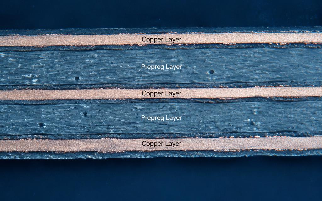
A common four-layer arrangement places signals on the outer layers with a solid ground plane and a power layer inside. Close coupling between signal layers and a ground reference minimises loop area and radiation.
Grounding strategy
For most mixed-signal boards, a single continuous ground plane with careful component partitioning works better than split grounds. Analog and digital sections are kept physically apart so that their return currents do not overlap.
Controlling emissions
- Keep fast edges no faster than needed
- Route clocks short and over solid reference
- Filter and decouple at every supply entry
- Avoid traces along board edges
Improving immunity
Interfaces leaving the board are the main entry points for disturbances. Filtering, TVS protection and proper shield termination at connectors keep external energy from reaching sensitive circuitry.
Frequently asked questions
Working on something similar?
Tell us about your application and we'll respond with practical engineering next steps.
Have a custom electronics project in mind?
Share your requirements and get a structured engineering response from our team.