
PCB Design · 3 min read
Schematic to PCB: Custom Board Development Workflow
What actually happens between 'we need a board' and holding the first prototype — and where the important decisions are made.
NANOSOFT Engineering Insights
Architecture before schematic
A block diagram defines the functional blocks, power domains and interfaces. It is the place to decide, for instance, whether the analog front-end needs its own supply or whether a bus should be isolated.
Schematic capture and component selection
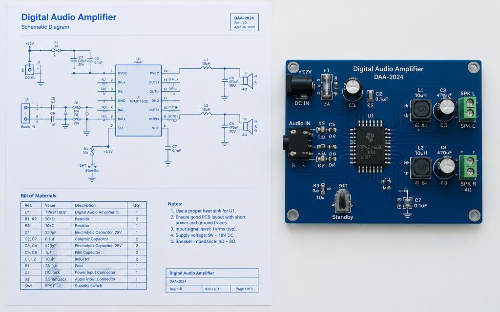
Each block becomes a circuit. Components are chosen for function, tolerance, availability, footprint and cost. Good schematics are readable: logical page structure, clear net names and notes explaining non-obvious choices.
Design review
Before layout, the schematic is reviewed against requirements and datasheets. Power sequencing, pin assignments, protection and test points are checked. Catching an error here costs minutes; catching it after fabrication costs a board spin.
PCB layout
Stack-up and placement
Layer count, ground planes and component placement are set by signal, power and mechanical needs.
Routing
Critical nets are routed first: sensitive analog, high-current paths and fast digital signals.
DFM checks
Clearances, annular rings, solder-mask and panelisation are checked against the manufacturer's capabilities.
Outputs and prototype
Prototypes are then built and brought up, and findings feed back into the next revision.
- Gerber and drill files
- Pick-and-place and assembly drawings
- Bill of materials with manufacturer part numbers
- Fabrication notes and stack-up
Frequently asked questions
Working on something similar?
Tell us about your application and we'll respond with practical engineering next steps.
Have a custom electronics project in mind?
Share your requirements and get a structured engineering response from our team.