
PCB Design · 3 min read
Common PCB Layout Mistakes and How to Avoid Them
Most board re-spins trace back to a handful of avoidable layout errors. Here are the ones we look for first.
NANOSOFT Engineering Insights
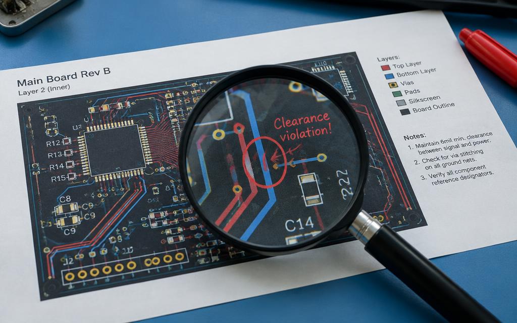
Broken return paths
Every signal current returns to its source. Slots or splits in a ground plane under a trace force that return current to detour, creating loops that radiate and pick up noise. Keep reference planes continuous under critical signals.
Decoupling placed too far away
A decoupling capacitor only works if the loop between it, the IC power pin and ground is short. Place small-value capacitors as close as possible to the pins, with direct vias to the plane.
Ignoring thermal behaviour
Power components need copper area, thermal vias and airflow. A regulator that is fine on the bench may overheat in a sealed enclosure.
Clearance and creepage
High-voltage sections need adequate spacing, slots where necessary and attention to the applicable safety standard. These are not cosmetic — they determine whether a product can be certified.
Assembly and test oversights
- Missing fiducials or poor panelisation
- Components too close for rework
- No accessible test points for production test
- Inconsistent polarity markings on silkscreen
Frequently asked questions
Working on something similar?
Tell us about your application and we'll respond with practical engineering next steps.
Have a custom electronics project in mind?
Share your requirements and get a structured engineering response from our team.